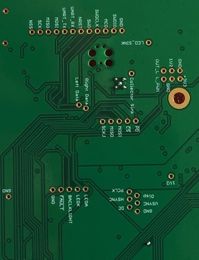
Whether it be your first printed circuit board (PCB) design or your hundredth, each has its own challenges when it comes time to get it manufactured. Often this area of electronics design is overlooked and can become quite a large headache if issues arise. There are many different types of potential problems that exist, which are largely dependent on the size of the components, thermal requirements and package technologies used in the design. A quick review of the circuit board layout plan early on in the process will generally yield an easier to manufacture design.
When starting a circuit board layout, the first step usually is to create the actual component footprints themselves. It may seem counter intuitive to reach out to a manufacturer at this point in time before any work has been done, but if you have a concrete plan of the general component sizes you are thinking of using they may be able to provide their recommended footprint(s)/guidelines at that time so it can be designed in as early as possible. Along with this, it is often a good idea to inquire about the intended manufacturer’s process capabilities. If the manufacturer’s process does not support the necessary placement, inspection and rework capabilities for a given package technology, it generally is a good idea to identify other manufacturers that have this capability or migrate package technology to a more forgiving/easier to solder type. It is helpful to categorize the components used in the design from highest risk to lowest with regards to solder ability. This makes it easy to focus efforts to the most likely parts to cause problems and spend extra time searching through the part manufacturer’s documentation to see what recommendations they have related to the footprint.
The next part of the design is to actually lay out the circuit board components/traces. Best practice with regards to component placement is to avoid crowding them too close together or locating them too close to the edge of the board. This helps alleviate the risk associated with high component density and/or component dislocation during the various manufacturing steps. Another key area to focus on is the manufacturing requirements for the bare PCB itself. Most standard board fabrication processes have several key requirements when it comes to trace/space widths, via hole size and copper features near the edge of the board. These aspects of the layout need to be kept in consideration throughout the design, review and quoting process.
When working on designs with a large number of power electronics and thermal design constraints, some other issues arise during the solder reflow process. If there is a high concentration of large thermal capacity components (e.g. parts with large thermal pads/slugs such as power MOSFETs, integrated DC/DC converters and RF modules), it can cause uneven heating during the solder reflow process. This can lead to cold solder joints, where nearby components are not securely soldered, or tombstoning, where the component stands on end and only one side makes contact with the solder pad. These issues are generally avoided by keeping smaller components away from large thermal components in the design or by refining the reflow oven profile with an instrumented board of the actual design to ensure even heating across the board area. Other situations where thermal design can hinder the soldering process is when thermal vias are employed. These vias sole purpose are the channel heat from one side of the board (often a thermal pad underneath an IC) to the other to interface with a large copper area or heatsink. There are good, better and best design practices when it comes to via in thermal pad design:
Good: Tented vias with solder mask
- This tend to be the lowest cost option. It involves intentionally filling the via holes with solder mask. In practice, it can cause issues with outgassing when the reflow heat is applied. This escaping gas can cause significant voids beneath components, reducing the effective thermal path. Careful via spacing and stencil design can help reduce the risk with this strategy.
Better: Reducing the size of the thermal vias
- If the PCB fab house allows, reducing the thermal vias down to 0.008” can help to prevent most issues with soldering, mainly solder wicking from beneath the part via capillary action. Generally, with 0.012” via diameter and up, excessive solder wicking will occur and voiding/poor thermal transfer will result.
Best: Plated filled vias
- In practice, this is the most expensive option. It involves filling the vias with a conductive epoxy then plating over them by and electrochemical deposition process. This greatly reduces the risk of solder voiding and creates the best thermal conduction path through the PCB.
Note: The above practices are mainly applicable for large thermal pads, BGA lands should only follow the “Best” practice to ensure reliability.
The circuit board/assembly designer has many freedoms throughout the component selection, arrangement and layout process. This is a double edge sword as it can lead to a design that is difficult to manufacture and/or exhibits reduced reliability once deployed into the final product. Careful planning and early coordination with the intended manufacturer is the lowest risk path to ensure a smooth transition from small engineering level builds to mass production.
Interested in learning more about Boulder Engineering Studio? Let's chat!
Previous Blog Posts
PCB Silkscreen: Consider your Stakeholders |
Building Raspberry Pi Disk Images with Docker |

|

|
.svg)


